Master Patterns for Phototooling (Masks), one-of-a-kind deliverables (Master as Part), and Replications are produced by EITHER:
|
|
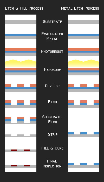
1. "ETCH AND FILL PROCESS": Etching the pattern within the substrate surface and filling the etched areas with an opaque fill:
PROCESS STEPS
- Glass substrate is procured, inspected, and cleaned.
- Metal Coating applied.
- Light Sensitive Photoresist applied by spin coating or dip coating.
- Exposure of the Photoresist pattern by AUTOGRAPH or contact print of a Photo Tool or Mask.
- Develop Photoresist and Inspect for its masking quality. Areas to be removed will be exposed after Developing.
- Chemically Etch Metal Coating in exposed areas. Inspect remaining metal/photoresist areas for masking qualities.
- Chemically Etch Glass substrate. Inspect etched areas for quality.
- Strip or remove both Photoresist and Metal Coating layers.
- Fill etched areas within substrate surface with epoxy or other opaque Fill material.
- Temperature or air cure filled areas of pattern.
2. ETCHED METAL (primarily Chrome) ON SUBSTRATE PROCESS: Metal is evaporative or sputter coated onto the substrate and the clear areas are etched away:
PROCESS STEPS:
- Glass substrate is procured, inspected and cleaned.
- Metal Coating is applied. Methods included evaporation, sputtered deposition, electron beam,CVD, and others. Typical for Chrome coating Thin Film Thickness 1200-2000 Å.
- Light Sensitive Photo Resist applied by spin coating or dip coating.
- Exposure of the Photoresist pattern by AUTOGRAPH or contact print of a Phototool or Mask.
- Develop Photoresist and Inspect for its masking quality. Areas to be removed will be exposed after Developing.
- Chemically Etch Metal Coating in exposed areas.
- Strip or remove Photoresist leaving the Metal Coating layer on the substrate surface.
|